FSM State Assignment for Low Power and Power Estimation Under User-Specified Input Sequences

M.Koegst, G.Franke, K.Feske

FhG IIS Erlangen - Department EAS Dresden
Zeunerstr. 38
D-01069 Dresden, Germany

e-mail: koegst@eas.iis.fhg.de


Introduction

   Power dissipation is becoming a critical parameter in the design of microelectronic circuits, especially in portable applications. Therefore a low power design of FSMs implies the necessity of adapted minimization approaches at both technology-independent and technology-dependent level of specification and moreover the possibility of an acceptable power estimation for a synthesized circuit.

   In the literature different approaches and synthesis meth ods are published [DeM-95]. At the logic level there are three main viewpoints for power minimization: factorization including restructuring [RoB-93], state assignment [BeM95] and logic minimization [SSL-92].

   The goal of our paper is to present a new FSM state assignment procedure for low power and to demonstrate our strategy for low power design and power estimation with regard to user-specified input sequences.

State Assignment for Low Power

   Our procedure for state assignment aims at diminishing the switching activity of state transitions. We do it by mini mization the number of state variables that switch when the FSM changes between two adjacent states. This leads to a smaller power dissipation of the synthesized circuit.

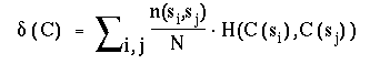
   In generalization of [RoP-93] we define for a given FSM the register switching rate d(C) for its state assignment C with regard to a given input sequence of the length N by

(Figure)

where are n(si,sj) the number of transitions between the states si and sj and H the Hamming distance of codes.

Our state assignment procedure consists of following steps:

  1. Computation of a code C by simulated annealing using d(C) as a measure of code quality.
  2. Improving of C by negation of selected state lines.
  3. Modification of the code using don`t cares.

Strategy for Design and Power Estimation

   We apply a strategy for low power design and power esti mation consisting of four main steps (s. Figure 1):

  1. State encoding for low power with regard to an input sequence.
  2. Minimization of the encoded FSM and mapping at the given library (lca10k.genlib).
  3. Extending the given sequence of the primary inputs for the power simulation utilizing an adapted procedure of SIS [SSL-92, MDL-94].
  4. Power estimation of the synthesized circuit by simula tion with regard to the extended sequence.

(Figure)

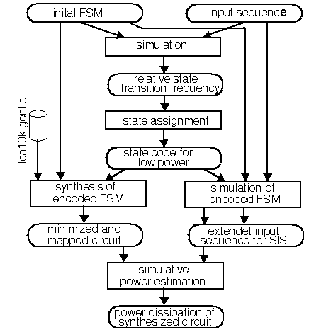
Figure 1   Strategy for design and power estimation

Experimental results show the effectiveness of our state assignment procedure for reducing the power dissipation.


References (subset)

[BeM-95] Benini,L.; de Micheli,G.: State Asignment for Low Power Dissipation. IEEE Journal fo Solid-State Cir cuits, Vol. 30, No. 3, March 95, pp. 32-40.

[DeM -95] Devadas,S.; Malik,S.: A Survey of Optimization Tech niques Targeting Low Power VLSI Circuits. 32th DAC, 1995, pp. 242-247.

[MDL-94] Monteiro,J.; Devadas,S., Lin,B.: A Methodology for Efficient Estimation of Switching Activity in Sequential Logic Circuits. 31th DAC, 1994, pp. 12-17.

[MKD-94] Monteiro,J.; Kukula,J.; Devadas,S.; Neto,H.: Bitwise Encoding of Finite State Machines. International Confer ence on VLSI Design, Calcutta, India, January 1994, pp.379-382.

[RoP-93] Roy, K.; Prasad, S. C.: Circuit Activity Based Logic Synthesis for Low Power Reliable Operations. IEEE Trans act. on VLSI Systems, vol. 1, No.4, Dec. 1993.

[SSL-92] Sentovich,E.; et.al.: "SIS: A System for Sequential Circuit Synthesis", Memo UCB/ERL M92/41, University of Berkeley, CA, 1992


Have a look to http://www.eas.iis.fhg.de/syn/home.html